Memory sub-
The memory unit is a
critical component of digital computing where data needs to be read, processed and stored frequently. Following block diagram shows the connectivity of CPU, memory and I/O unit through bus connections. As the requirements of storage capacity increases with the processing power of CPU, we need to design systems with several levels of storage. These levels of hierarchy requires several tradeoffs on design platform. One such tradeoff is with distance of the memory from CPU. As the distance increases, the delay on data transfer increases which in-Block diagram below shows the connectivity of CPU, memory and I/O unit through bus connections. Memory needs to be organized around CPU and central bus-
data communication in-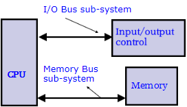
We have already covered CPU in previous section. Lets discuss the memory sub-
Computer memories are divided into Cache memory, main memory and secondary memory. Where Cache is the
fastest and closest to processor. Cache memory is also the smallest memory. Secondary memory is the slowest, furthest from processor and largest in size.

In next section we will discuss Cache memory organization. NEXT
Hope you liked! this page. Don't forgot to access relevant previous and next sections with links below.